First of all, I would like to thank Jonathan Clark, the author of the excellent reverse engineering project of the RPi Zero 2 W PCB, which has been extremely helpful in making this modification possible.
As many of you already know, the Raspberry Pi Zero 2 W actually has two UARTs inside the SoC, but only one of them is exposed to the GPIO header via pins GPIO14–15. Many users get confused about whether the second UART can be enabled and used. Let’s clarify this first: in stock configuration, the RPi Zero 2 W cannot use both UARTs simultaneously.
Let’s take a closer look at the BCM2835 pin function documentation to understand why.
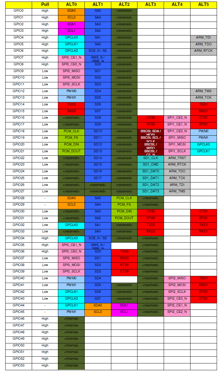
As seen in the table above, the chip provides multiple UART-capable pins (TXD0-1 and RXD0-1). However, on the Pi Zero 2 W header, only GPIO14–15 are routed. This means that whichever UART we use, the only useful external pins are GPIO14 and GPIO15. Now that this is clear, let’s explore how we can work around it.
 Warning
This modification involves soldering and PCB trace work, which can permanently damage your Raspberry Pi Zero 2 W if done incorrectly. Only attempt this if you have adequate soldering skills and experience. I am not responsible for any damage or malfunctions resulting from this procedure.
Why I Did This Modification?
In my case, I’m running Klipper host on a Raspberry Pi Zero 2 W for my Ender 3 V2 3D printer. The mainboard uses a CH340 USB-to-UART bridge, and I constantly had driver issues with it under Linux. To avoid these problems, I needed to connect directly to the mainboard’s UART interface instead of relying on USB.
At the same time, I also wanted to keep using the stock Ender 3 V2 screen (DWIN_LCD), which also communicates over UART. This meant I needed access to two independent UARTs on the Pi Zero 2 W — one for the mainboard and another for the screen.
That was the main motivation behind this whole project.
Following the PCB Traces
Thanks to Jonathan Clark’s reverse-engineered PCB layer images, we can trace the BGA balls and see exactly where each UART pin is connected.
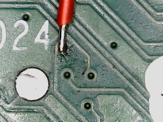
I first selected one pair of pins that already has UART functionality — the ones used by the onboard Bluetooth chip (not routed to the header). By tracing these pads from the top layer down through the vias, I found that they do not connect to inner layers before reaching the Bluetooth module. Instead, they pass through a via straight down to layer 6 (bottom), then back up to the top layer under the Bluetooth IC.
This is very fortunate, because it means we can “harvest” these UART pins with a bit of soldering, a few wires, and some careful work. Below you can see images of the BGA ball map and the UART trace locations on layer 1 and layer 6.
I have highlighted the UART pins with green and red boxes in both the BGA map and the layer images.


Re-routing the UART
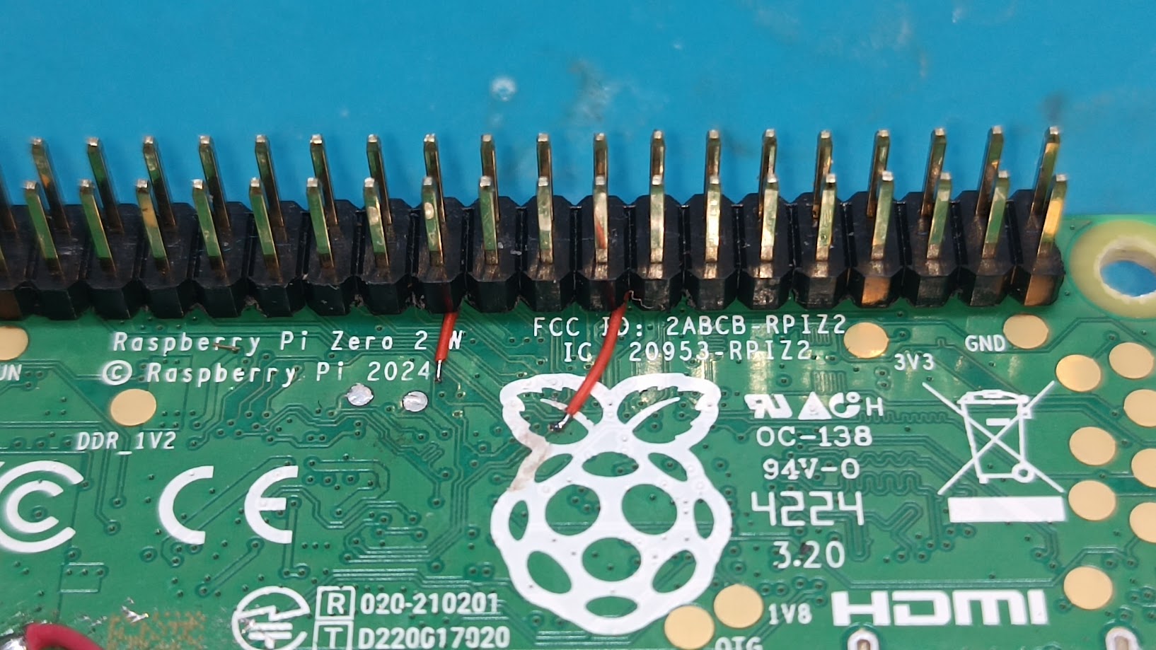
I chose to re-route these harvested UART signals to GPIO23–24 pins on the header. I picked these because they have fewer alternative functions and are less likely to be required in my projects. Below you can see the soldered wires from the vias to the GPIO23–24 header pins.


What about the original GPIO23–24 signals?
If we never configure GPIO23–24 as OUTPUT, they will remain in High-Z state and electrically harmless. However, as an extra precaution, you can cut the original traces to GPIO23–24. Conveniently, these traces are also located on layer 6, making them easy to isolate if needed.
There is one more conflict to address: GPIO32–33 are already connected to the Bluetooth chip. But we can solve this by disabling the WLAN_BT_REG_ON signal. When this pin is pulled low, the BT chip shuts down its Bluetooth interface and leaves the UART pins floating, freeing them up for our own use.
Configuration
Now let’s configure the overlays. Open:
sudo nano /boot/firmware/config.txt
Add the following lines at the end of the file (if not already present):
enable_uart=1
dtoverlay=disable-bt
dtoverlay=uart1,txd1_pin=32,rxd1_pin=33
dtoverlay=uart0,txd0_pin=14,rxd0_pin=15,pin_func=4
-
dtoverlay=disable-btdisables the WLAN_BT_REG_ON output, which effectively turns off the Bluetooth chip’s UART interface and leaves its pins in a floating state.This allows us to use the Pi’s GPIO32–33 pins for a second UART without having to physically disconnect them from the Bluetooth chip. -
The second and third overlay lines reassign UART0 and UART1 to their new pin mappings.
After saving and rebooting, you should now have:
-
ttyS0 available on GPIO32–33 (which we remapped from GPIO23–24 header pins), and
-
ttyAMA0 available on GPIO14–15.
This way, both UARTs become usable at the same time.
You can also verify the UART pin assignments by running the following command in the terminal:
pinctrl
You should see output similar to this:
14: a0    -- | hi // GPIO14 = TXD0
15: a0    -- | hi // GPIO15 = RXD0
32: a5    -- | hi // TXD0/GPIO32 = TXD1
33: a5    -- | hi // RXD0/GPIO33 = RXD1
41: op -- -- | hi // WL_ON/GPIO41 = output
42: op -- -- | lo // BT_ON/GPIO42 = output
This confirms that the TXD and RXD functions have been correctly assigned to the new pins, and that the WLAN_BT_REG_ON output has been disabled.
After completing all modifications, you can perform a loopback test by connecting the newly assigned GPIO32–33 pins together. Send characters through the UART and check if they are correctly received. If successful, the UART is ready for use.
Note:
-
ttyS0uses the mini-UART, which has some limitations and its baud rate may fluctuate depending on the CPU clock. -
ttyAMA0is the full-featured UART and should be preferred for critical peripherals like Klipper. -
In my setup, I run the DWIN LCD via
ttyS0.